Self-Aligned Oxide Thin Film Transistors and Its Circuit Operation
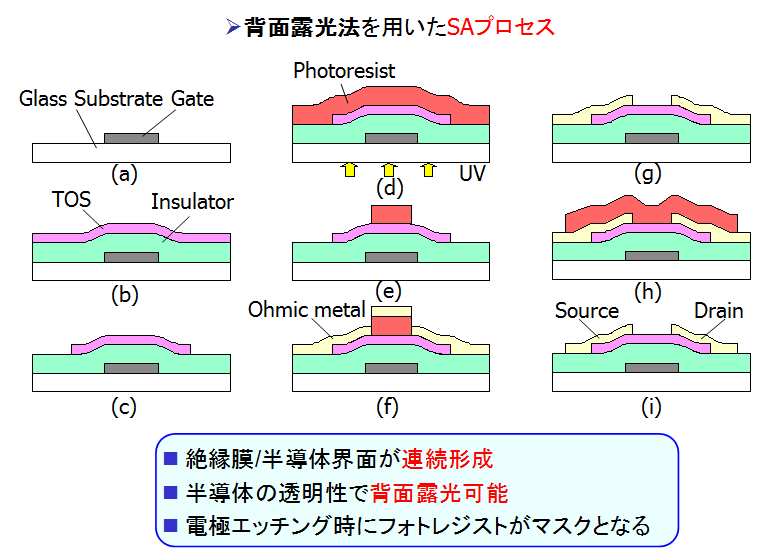
Transparent-oxide-semiconductor-based self-alignment thin-film transistors (TFTs) fabricated by a back-surface exposure method were investigated.
The alignment margin of the source and drain electrodes against a gate electrode was minimized.
The length of the overlapping region between the gate-source and gate-drain electrodes was as small as 0.9 μm.
The field-effect mobility, on-off ratio, threshold voltage, mutual conductance, and subthreshold slope were 4.3 cm2/Vs, 108, +0.5 V, 2.93 mS/mm, and 0.25 V/decade, respectively.
Combined with the mutual conductance 0.88 mS and capacitance 2 pF, the estimated cutoff frequency was 70 MHz.
A level-shift inverter with a super-buffer configuration, where a wide voltage margin and fast switching were expected, was fabricated.
The obtained gain and logic swing was 1.8 and 2.5 V, respectively.
- Y. Hirouchi, A. Yamagishi, S. Naka, and H. Okada: "Transparent-Oxide-Semiconductor-Based Self-Alignment Thin-Film Transistors", Jpn. J. Appl. Phys., 48(4), 04C097 (2009).
Copyright ©
Electronic Material and Devices Engineering Laboratory, University of Toyama.
All rights reserved.