Welcome
Welcome to Organic Optical Device Engineering Laboratory!
We investigate the optical devices and electronics with organic marerials.
Welcome to Organic Optical Device Engineering Laboratory!
We investigate the optical devices and electronics with organic marerials.
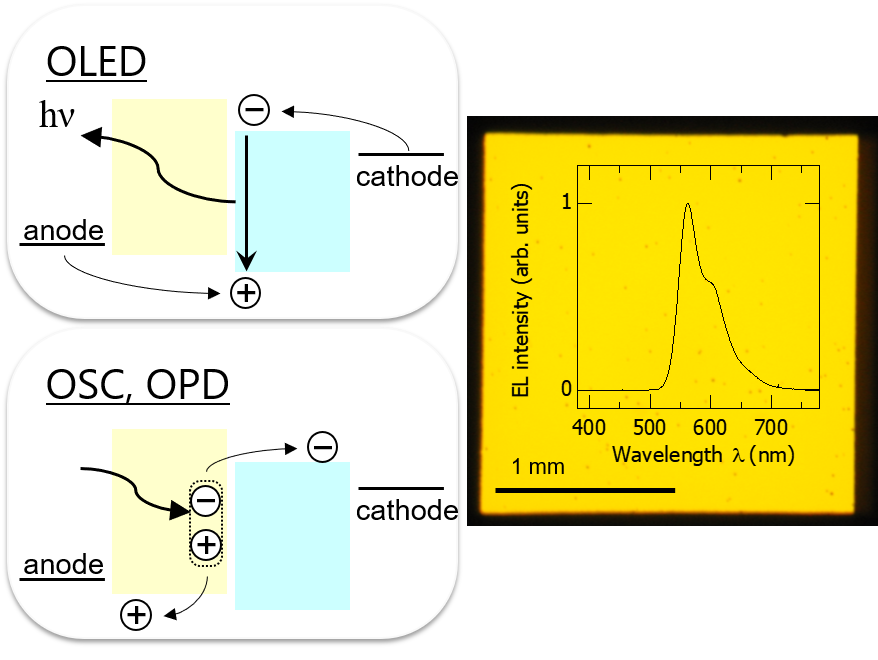
We have developed a Multi Functional Diodes (MFD) which can be used as both the light emitting and receiving devices with a single device structure. MFDs are expected to be applied to the solar cells in the daytime and the lighting for plant factories in the evening.
article
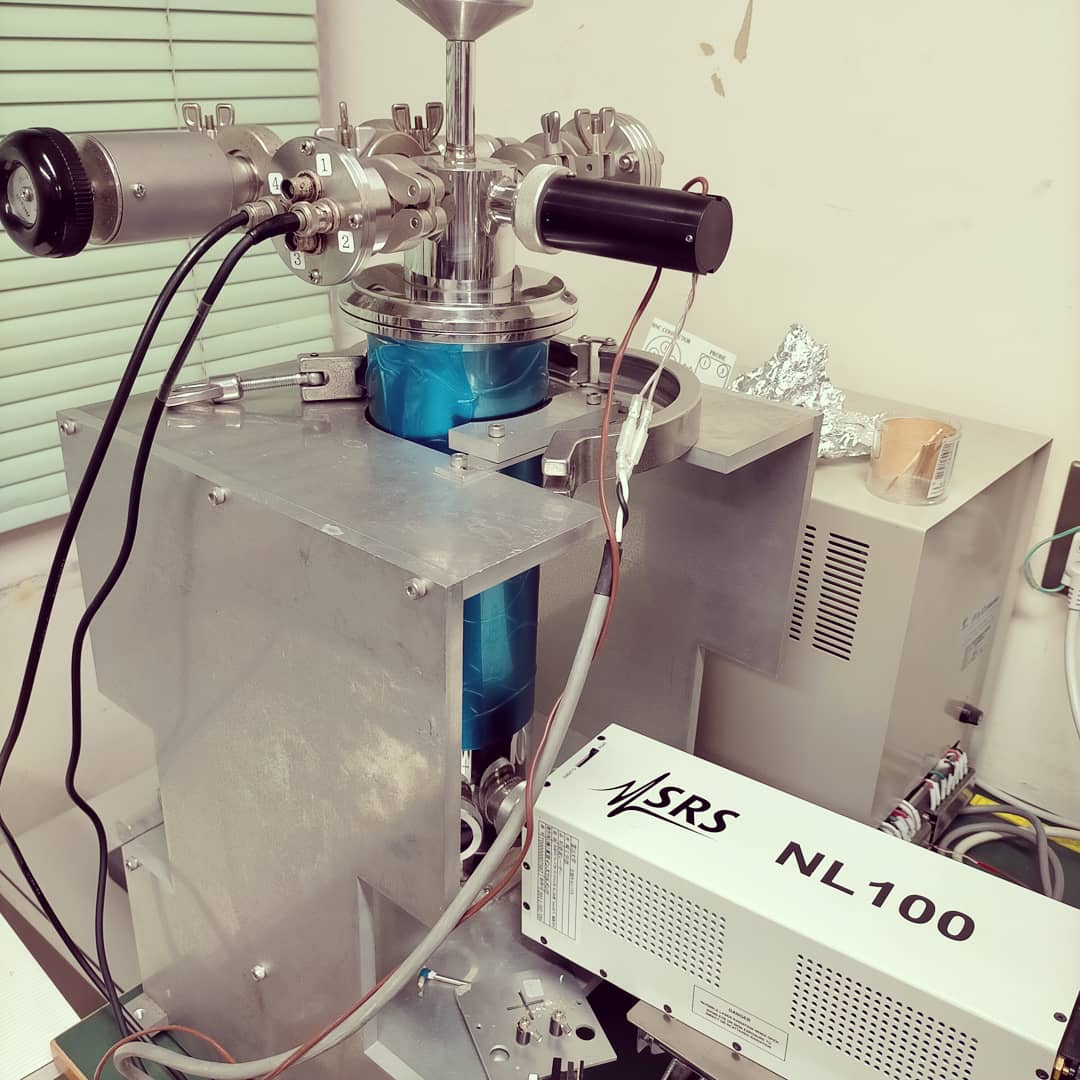
The charge mobility of organic semiconductors has been measured using a Time-of-Flight method and analysis of carrier injection at the electrodes-semiconductors interface.
article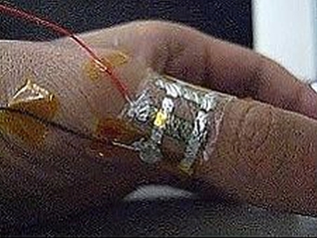
We have investigated an Ultra flexible OLEDs with 1 um thickness. This is expected to apply to a wide variety of microscopic shapes, i. e. the skin and so on.
movie
Prof. Naka
Assoc.Prf. Morimoto
one Technical staff
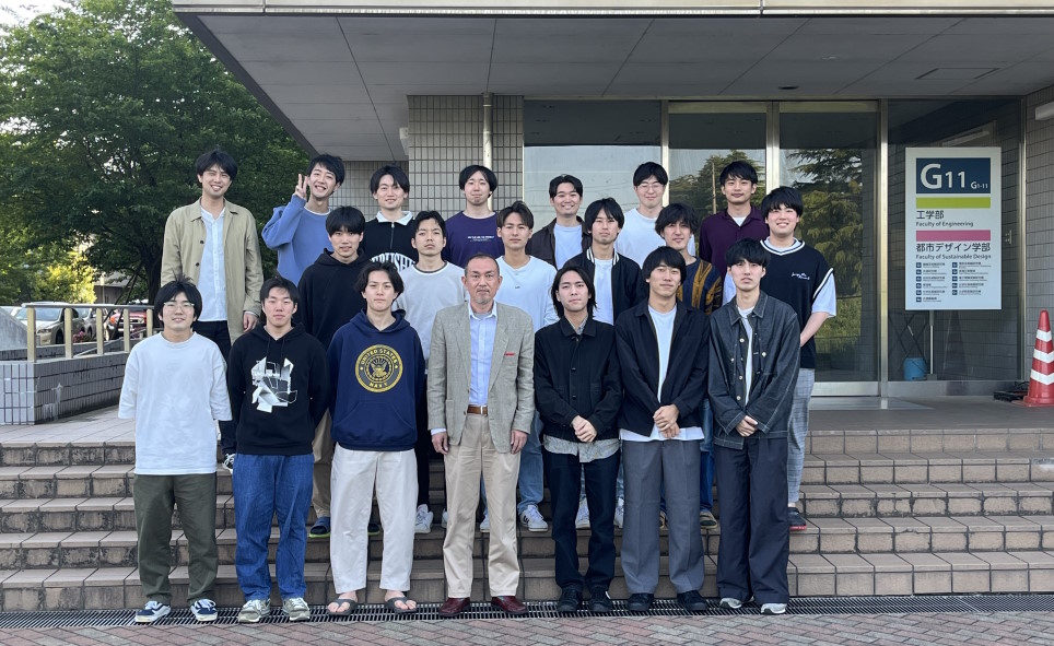
M2: 5 students
M1: 7 students
B4: 8 students
Our laboratory was established in April 2018 with keywords of organic, optics, and device. We will continue research and development new optical devices, process technologies, and fundamental device physics.
Fields
OLEDs, Organic Electronics, Optical Engineering
Academic Society Affiliations
The Japan Society of Applied Physics
The Institute of Image Information and Television Engineers
The Institute of Electronics
Information and Communication Engineers
I am researching the structural control of organic materials and application of next-generation electronics devices. In addition, I aim to coexist with humans and devices by using soft organic materials and naturally friendly biomaterials,
Fields
Organic Thin Films, Structural Control, OLEDs, Sensors
Academic Society Affiliations
The Japan Society of Applied Physics
The Society of Polymer Science Japan
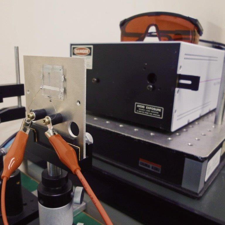
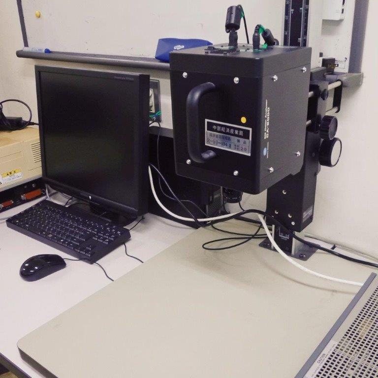
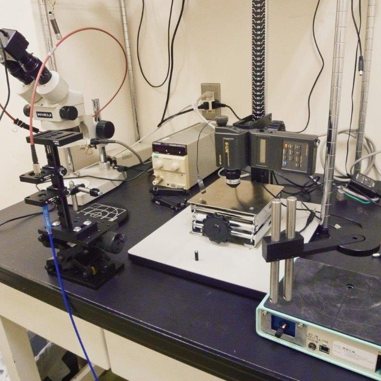
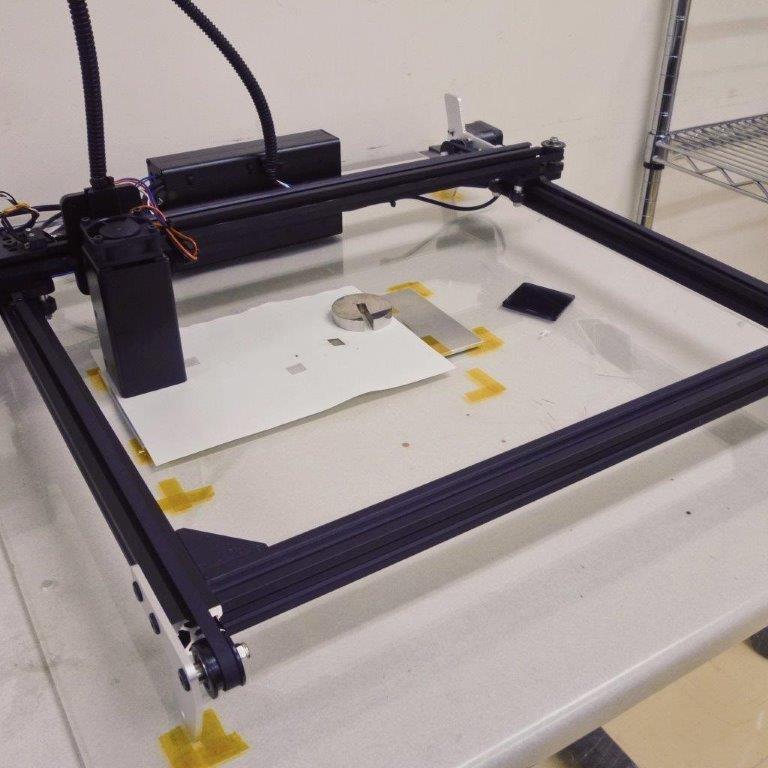
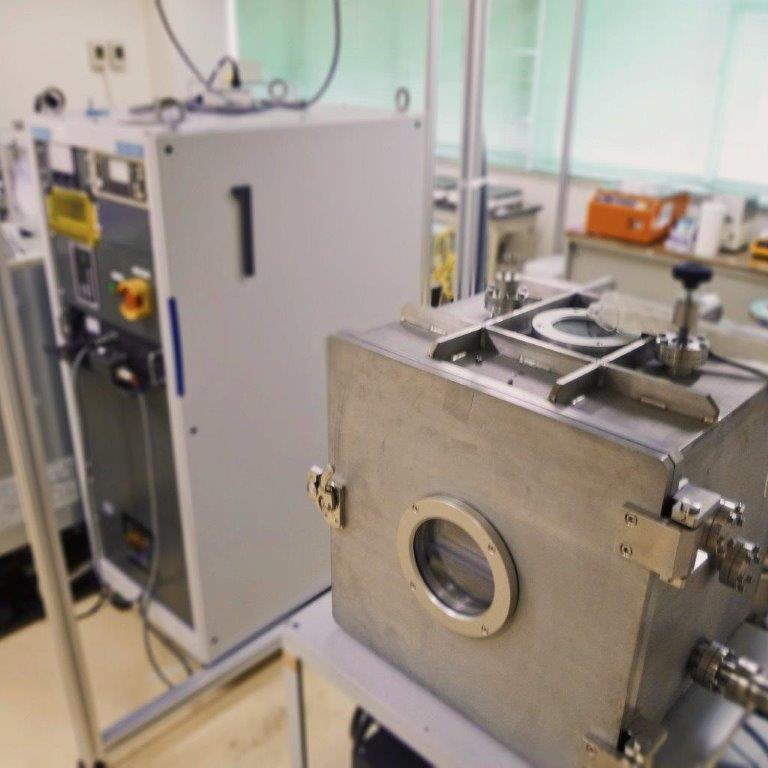
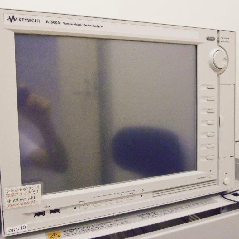
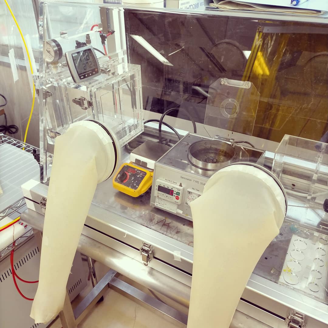
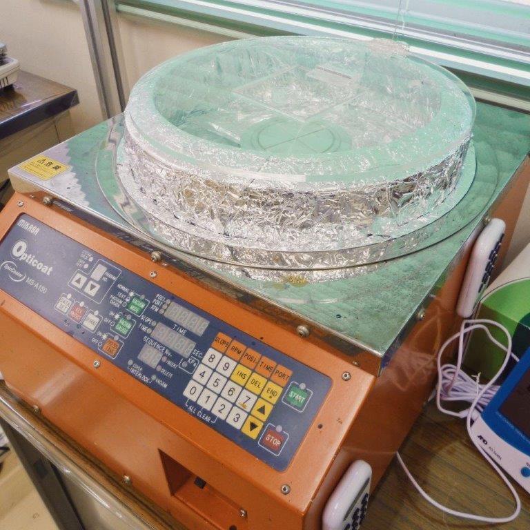
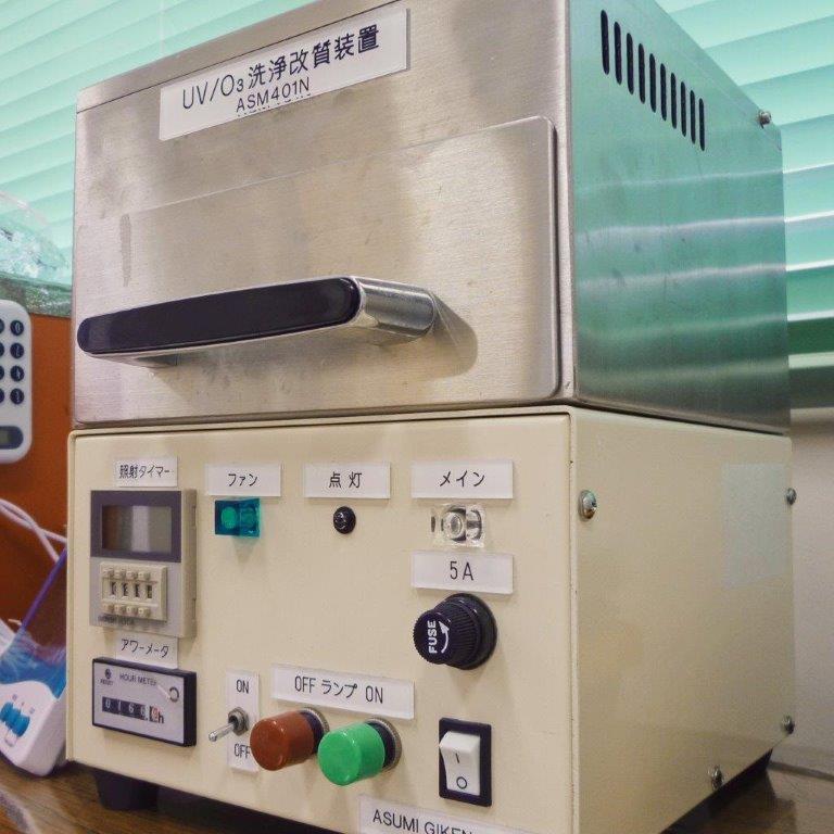
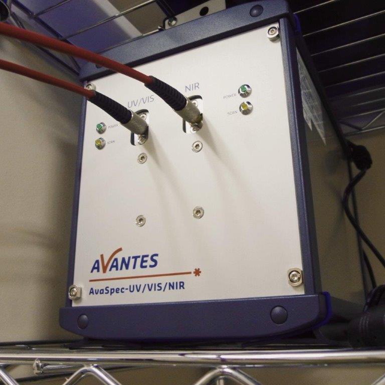
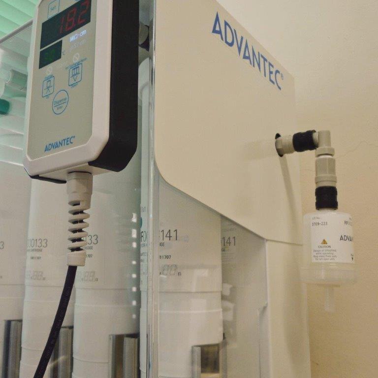
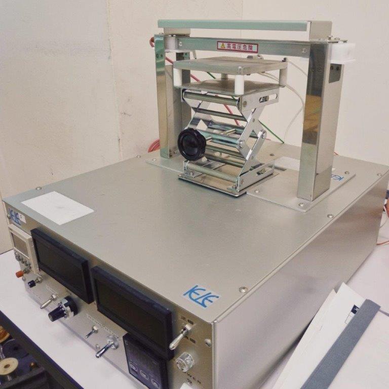
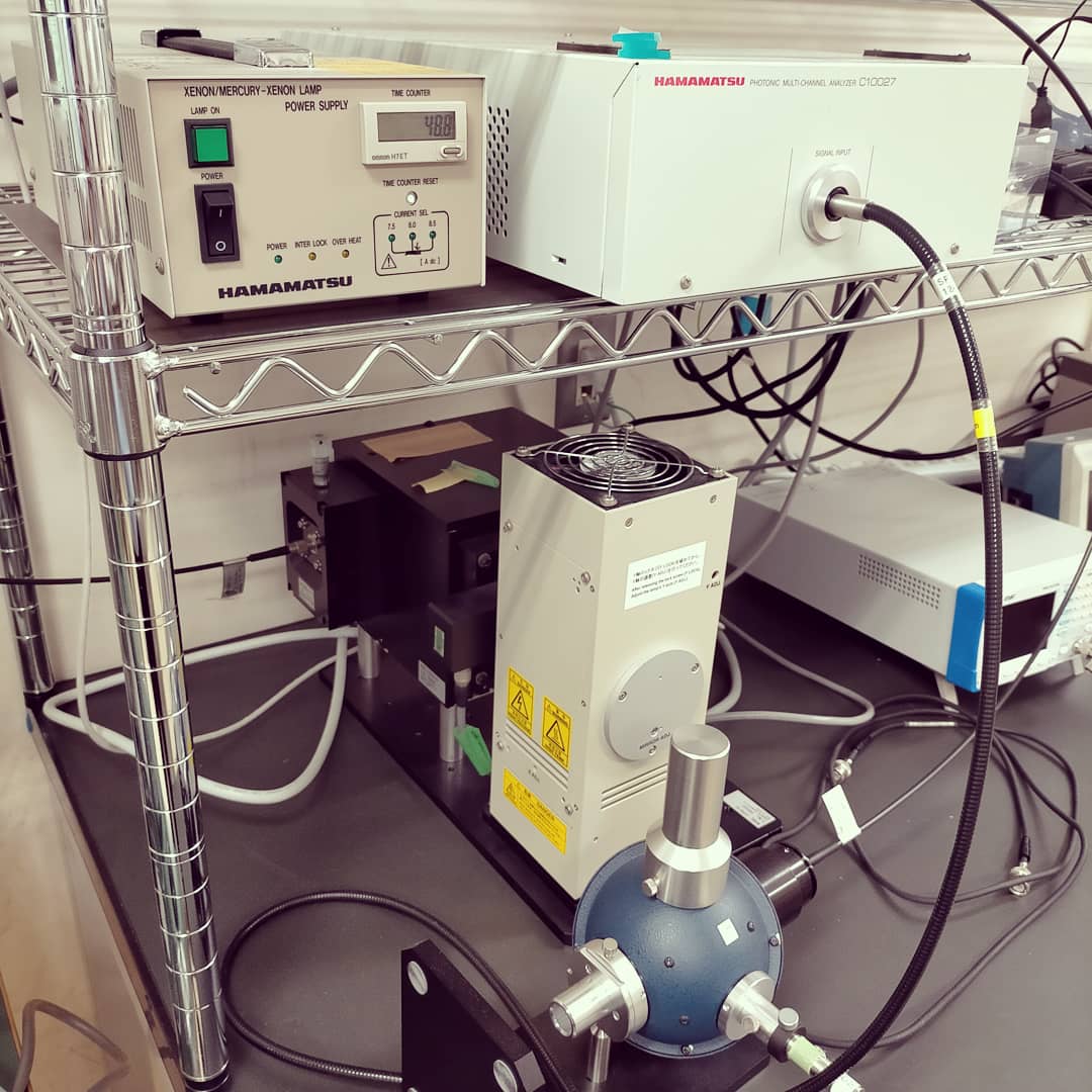
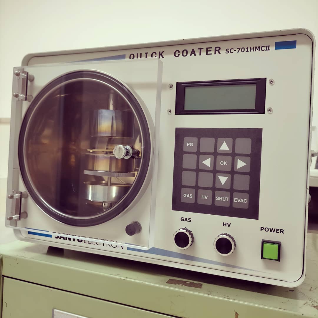
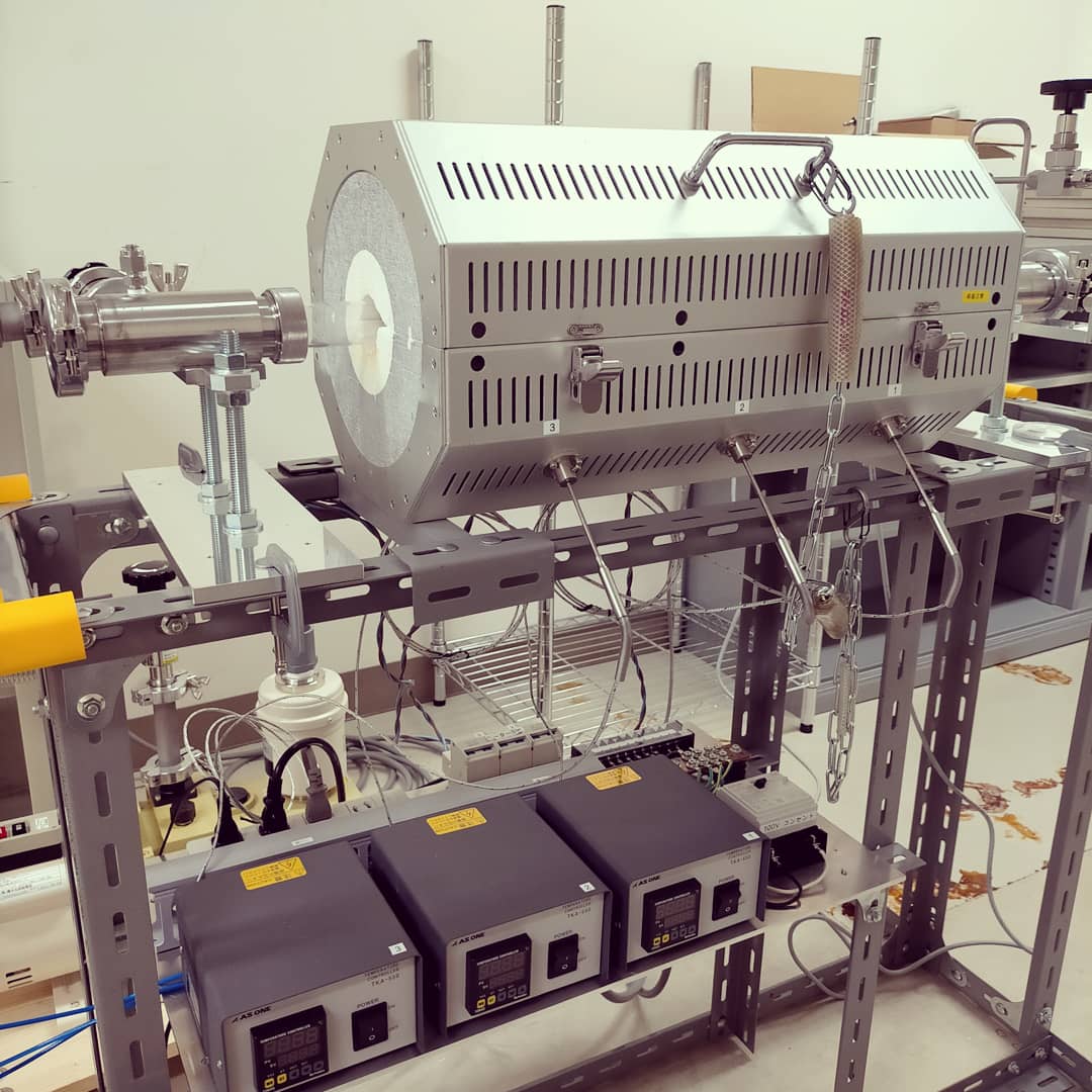
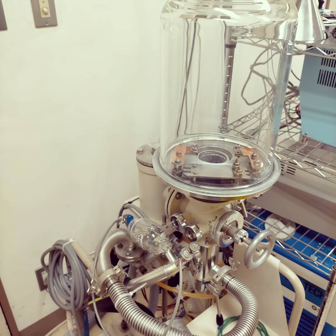
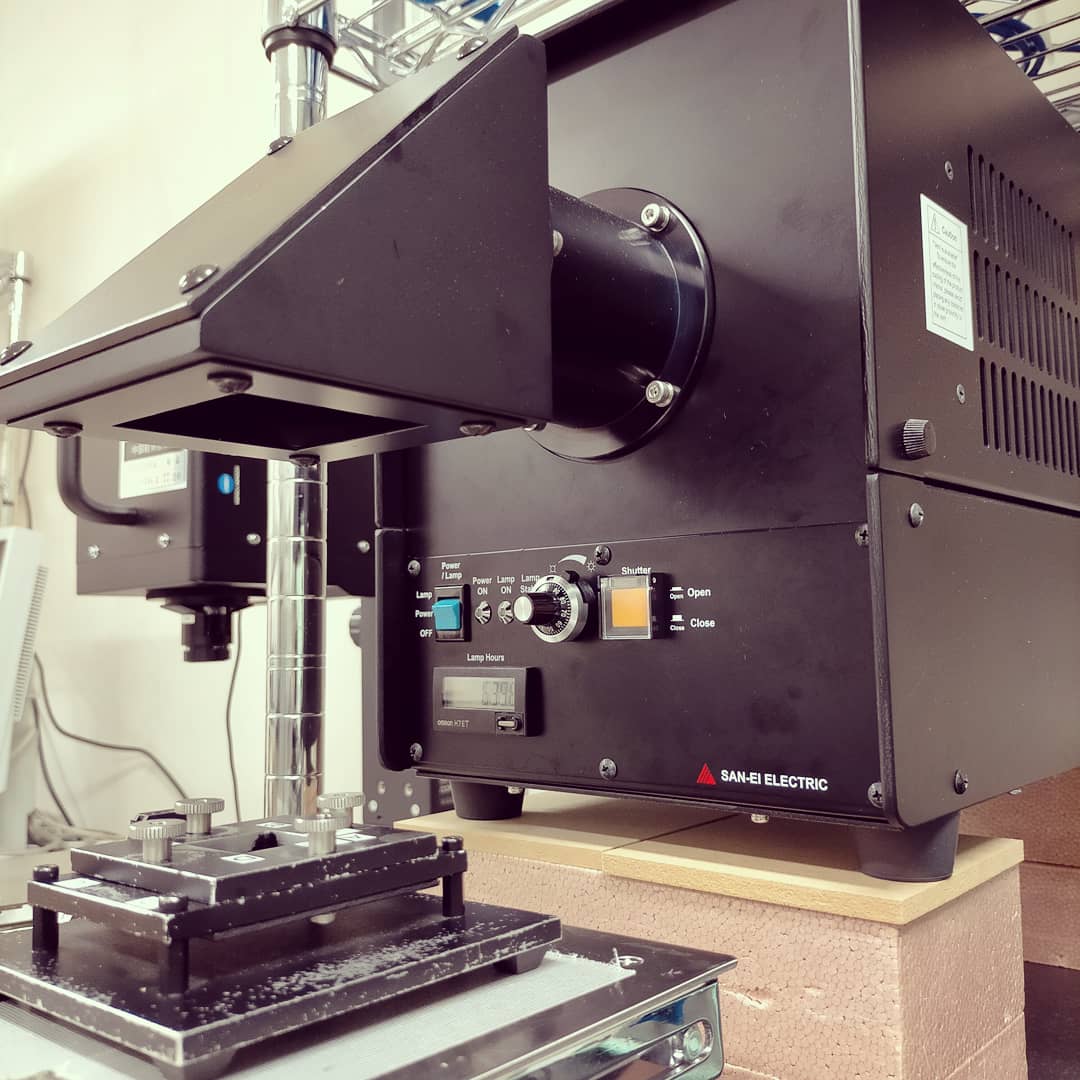
Noteworthy introduction such as OLEDs and Solar cell fabrication, evaluation equipments.
Please contact us by e-mail for collaborative research. Counseling on international student career is always accepted.